
No products in the cart.

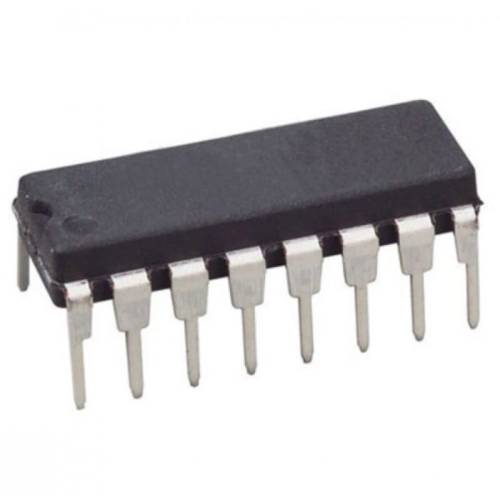
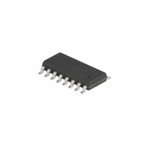
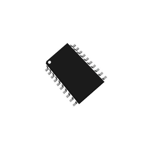
The 74HC151 high speed Digital multiplexer utilizes advanced silicon-gate CMOS technology. Along with the high noise immunity and low power dissipation of standard CMOS integrated circuits, it possesses the ability to drive 10 LS-TTL loads. The 74HC151 selects one of the 8 data sources, depending on the address presented on the A, B, and C inputs. It features both true (Y) and complement (W) outputs. The STROBE input must be at a low logic level to enable this multiplexer. A high logic level at the STROBE forces the W output HIGH and the Y output LOW. The 74HC logic family is functionally as well as pin-out compatible with the standard 74LS logic family. All inputs are protected from damage due to static discharge by internal diode clamps to VCC and ground.
Features:-
- Typical propagation delay data select to output Y: 26 ns
- Wide operating supply voltage range: 2–6V
- Low input current: 1 µA maximum
- Low quiescent supply current: 80 µA maximum (74HC)
- High output drive current: 4 mA minimum
Specification:-
| Symbol | Parameter | Value | Unit |
| VCC | Supply Voltage | ? 0.5 to + 7.0V | V |
| VIN | DC Input Voltage | ? 1.5 to VCC + 1.5V | V |
| VOUT | DC Output Voltage | ? 0.5 to VCC + 0.5V | V |
| IIK, IOK | Clamp Diode Current | ± 20 | mA |
| IOUT | DC Output Current, per pin | ± 25 | mA |
| ICC | DC VCC or GND Current, per pin | ± 50 | mA |
| TSTG | Storage Temperature Range | ? 65°C to + 150 | °C |
| PD | Power Dissipation | 500 | mW |
| TL | Lead Temperature | 260 | °C |
* product image for illustration purposes only. actual product may vary.
Only logged in customers who have purchased this product may leave a review.


Reviews
There are no reviews yet