

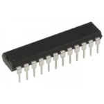
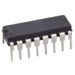
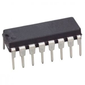
74LS173 4 bit D type Registers with 3 State Output IC (74173) DIP 16 Package
₹136.80 (incl. tax)
74LS173 4 bit D type Registers with 3 State Output IC (74173) DIP 16 Package
The 74LS173 is a quad (4-bit) D-type register with 3-state outputs and control features such as parallel load, clock enable, and output enable. It is part of the 74LS TTL (Low Power Schottky) logic family.
This IC is designed to store and transfer 4 bits of data under control of a clock signal. Data on the input lines (D0–D3) is latched into the register on the rising edge of the clock (CLK) when the clock enable inputs (G1 and G2) are LOW.
The outputs (Q0–Q3) can be enabled or placed in high-impedance (Hi-Z) state using the output control inputs (OE1 and OE2), allowing easy bus interfacing.
The 74LS173 provides fast switching speeds, high noise immunity, and low power consumption, making it ideal for use in microprocessor systems, data storage, and bus-oriented applications.
Click here to view related products
Features:-
- • 3-State Outputs Interface Directly With System Bus
- • Gated Output-Control LInes for Enabling or Disabling the Outputs
- • Fully Independent Clock Virtually Eliminates Restrictions for Operating in One of Two Modes: – Parallel Load – Do Nothing (Hold)
- • For Application as Bus Buffer Registers
- • Package Options Include Plastic Small-Outline (D) Packages, Ceramic Flat (W) Packages, Ceramic Chip Carriers (FK), and Standard Plastic (N) and Ceramic (J)
Specifications:-
| Symbol | Parameter | Min | Type | Max | Unit | |
| VCC | Supply Voltage | 4.75 | 5 | 5.25 | V | |
| TA | Operation free-air temperature | -5.2 |
| |||
| IOH | Output Current — High | 16 | mA | |||
| IOL | Output Current — Low | 0 | 70 |
|
Functional Description
- Data at D0–D3 is loaded into the register on the rising edge of the clock (CP) only when both enables G1 and G2 are LOW.
- When either G1 or G2 is HIGH, the register retains its previous data (no change).
- When MR (Master Reset) is LOW, all outputs are cleared to 0 asynchronously.
- The output enable inputs (OE1, OE2) control the state of Q0–Q3 outputs:
- When both OE1 and OE2 are LOW, outputs are active.
- When either OE1 or OE2 is HIGH, outputs go to high-impedance (Hi-Z).
Applications
- Microprocessor data latching and buffering
- Bus-oriented systems (with tri-state outputs)
- Parallel data storage / transfer
- Shift register expansion
- Memory data register
- Temporary data holding in digital systems
- I/O port register or latch
- Control and status register implementation
* Product image for illustration purposes only, actual product may vary.
Only logged in customers who have purchased this product may leave a review.
You may also like…
74HC595 8 bit Serial to Parallel Shift Register IC (74595) DIP 16 Package
₹23.00 (incl. tax)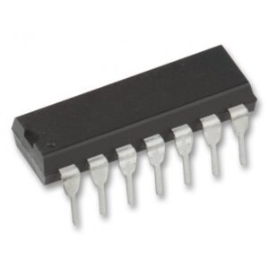
74HC08 Quad 2 Input AND Gate IC (7408) DIP 14 Package
₹14.40 (incl. tax)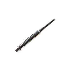
Normal Bit Tip for 25W Soldering Iron
₹32.00 (incl. tax)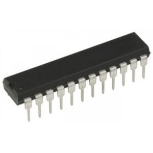
74LS154 4 Line to 16 Line Decoder/Demultiplexer IC (74154) DIP 24 Package
₹199.00 (incl. tax) 74LS147 Decimal to BCD Priority Encoder IC (74147) DIP 16 Package
₹64.80 (incl. tax)Related products
74HC221 Dual Monostable Multivibrator with Reset IC (74221) DIP 16 Package
₹26.40 (incl. tax) 74HC393 Dual 4 bit Binary Ripple Counter IC (74393) DIP 14 Package
₹23.00 (incl. tax) 74HC02 Quad 2 Input NOR Gate IC (7402) DIP 14 Package
₹16.80 (incl. tax)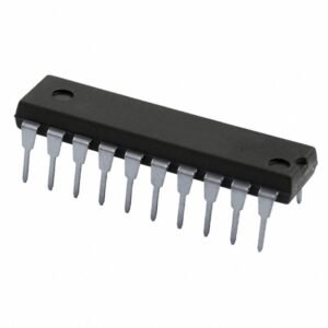
74HC573 Octal D Type Transparent Latch IC (74573) DIP 20 Package
₹30.00 (incl. tax) 74HC148 8 to 3 Line Priority Encoder IC (74148) DIP 16 Package
₹38.40 (incl. tax) 74HC374 3 State Output Octal D Type Flip-Flop IC (74374) DIP 20 Package
₹21.60 (incl. tax) 74HC240 Octal Buffer Line Driver IC (74240) DIP 20 Package
₹19.20 (incl. tax)
Reviews
There are no reviews yet