
No products in the cart.
74 Series SMD IC
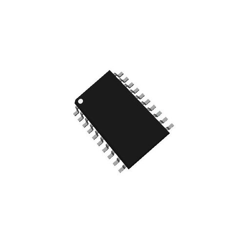
74HC540 IC – (SMD Package) – Octal 3-state Inverting Buffer IC (74540 IC)
₹42.00 (incl. tax)
The 74HC540 is identical in pinout to the LS540. The device inputs are compatible with Standard CMOS outputs. External pull?up resistors make them compatible with LSTTL outputs. The HC540A is an octal inverting buffer/line driver/line receiver designed to be used with 3?state memory address drivers, clock drivers, and other bus?oriented systems. This device features inputs and outputs on opposite sides of the package and two ANDed active?low output enables.
Features:-
- Output Drive Capability: 15 LSTTL Loads
- Outputs Directly Interface to CMOS, NMOS, and TTL
- Operating Voltage Range: 2.0 to 6.0 V
- Low Input Current: 1 A
- High Noise Immunity Characteristic of CMOS Devices
- In Compliance With the JEDEC Standard No. 7 A Requirements
- Chip Complexity: 124 FETs or 31 Equivalent Gates
- NLV Prefix for Automotive and Other Applications Requiring Unique Site and Control Change Requirements; AEC?Q100 Qualified and PPAP Capable
- These Devices are Pb?Free and are RoHS Compliant
Specification:-
| Symbol | Parameter | Value | Unit |
| VCC | Supply Voltage | ? 0.5 to + 7.0V | V |
| VI | DC Input Voltage | –0.5 to VCC + 0.5 | V |
| VO | DC Output Voltage | ?0.5 ? VO ? VCC + 0.5 | V |
| IIK | DC Input Diode Current | ±20 | mA |
| IOK | DC Output Diode Current | ±35 | mA |
| IO | Output Current | ± 35 | mA |
| ICC or IGND | DC VCC or GND Current, per pin | ± 75 | mA |
| TSTG | Storage Temperature Range | ? 65°C to + 150 | °C |
| PD | Power Dissipation | 500 | mW |
| TL | Lead Temperature | 260 | °C |
* product image for illustration purposes only. actual product may vary.
Only logged in customers who have purchased this product may leave a review.


Reviews
There are no reviews yet